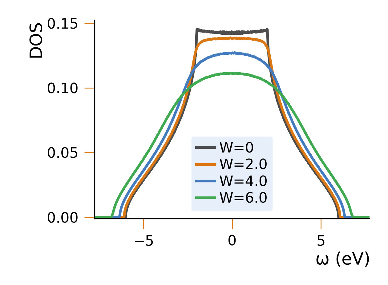
Density of states for a periodic cubic lattice. The system has size 501 x 501 x 501.
The onsite disorder is modeled by a random potential with a uniform distribution of
amplitude W. The results are averaged over the random potential distributions. The DOS is
obtained via stochastic evaluation of the expectation value of the DOS operator expanded
in Chebyshev polynomials.#
The DOS shows a broadening of spectral features with increasing disorder strength.
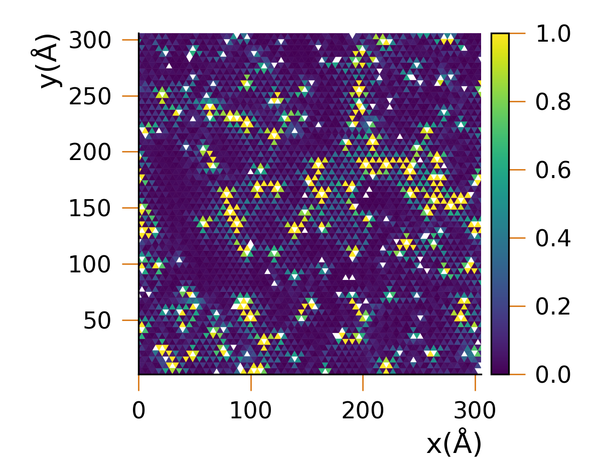
Spatially resolved LDOS at the Fermi energy \(E_F=0\). The graphene sheet has size
101x101 unit cells, with periodic boundary conditions and with a vacancy density of 4%.
Only a smaller view of the whole sheet is shown here.
Each triangle is the Voronoi cell associated with each site. White areas denote the defects.
The LDOS is obtained via the Green's function, calculated by means of a Chebyshev expansion
of the resolvent.
The colormap is clipped at a maximum value of 1 for plotting purposes.#
The LDOS shows peaks around vacancies and exhibits interference patterns across different
vacancies.
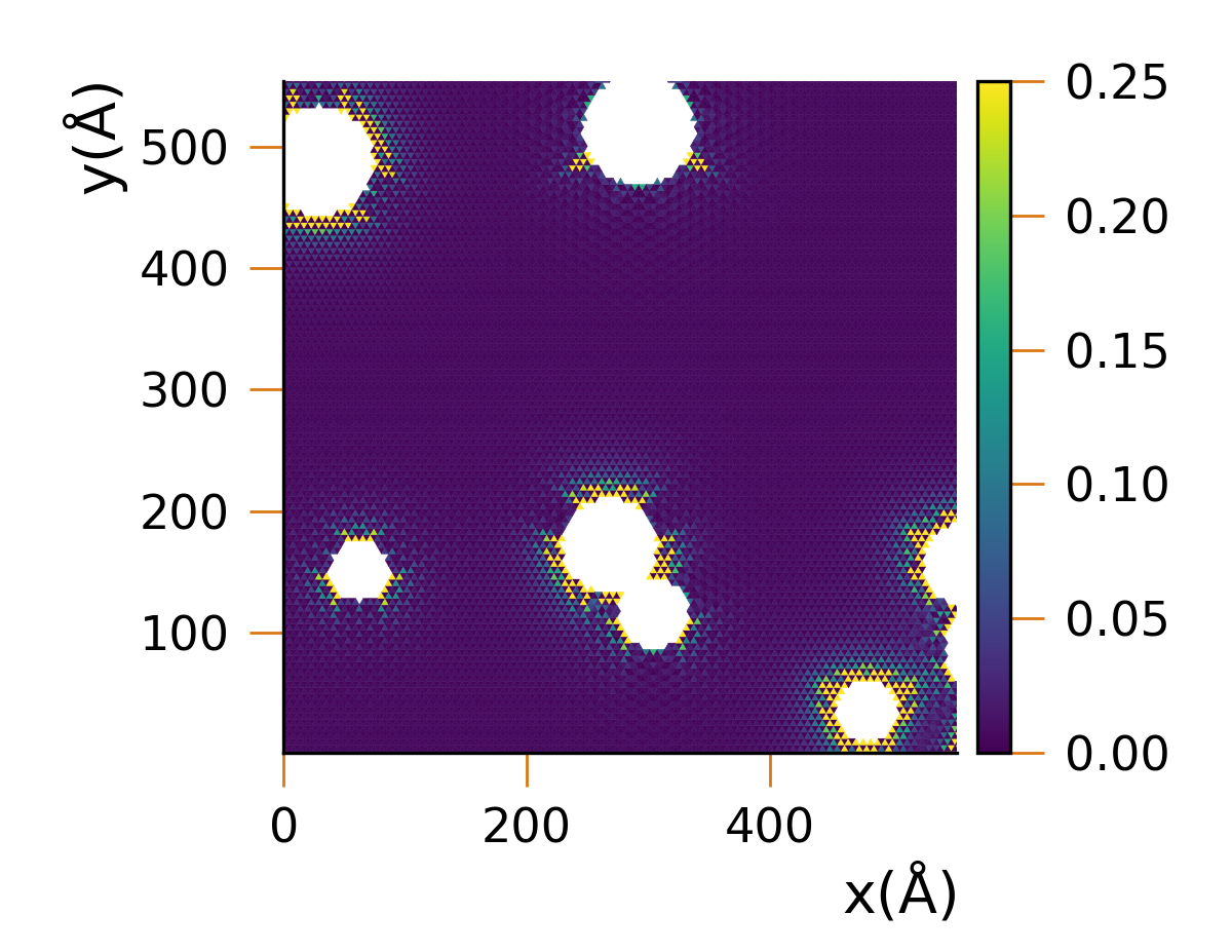
Spatially resolved LDOS at the Fermi energy \(E_F=0\). The graphene sheet has size
151x151 unit cells, with periodic boundary conditions and with few large circular defects.
Only a smaller view of the whole sheet is shown here.
Each triangle is the Voronoi cell associated with each site. White areas denote the defects.
The LDOS is obtained via the Green's function, calculated by means of a Chebyshev expansion
of the resolvent.
The colormap is clipped at a maximum value of 0.25 for plotting purposes.#
The LDOS shows increased spectral weight around the defects with symmetry depending on the
position within the unit cell of the center of the hole. The effect associated with the
structural irregularity is rather weak as there is little overlap, hence interference,
between different defects.
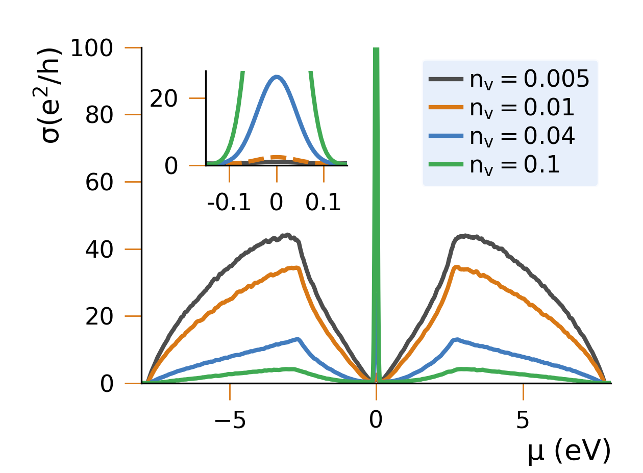
Electrical conductivity in the x direction \(\sigma_x\) as a function of the chemical
potential \(\mu\), for different vacancy densities. The graphene sheet has size
201x201 unit cells, with periodic boundary conditions.
The conductivity is obtained by evaluating the zero temperature Kubo-Formula via expansion
in Chebyshev polynomials.#
Increasing the vacancy density gradually reduces the conductivity of the system, except for
\(\mu=0\), which corresponds to half-filling, for which a delta-like peak appears.
The inset shows a zoom-in around this point.
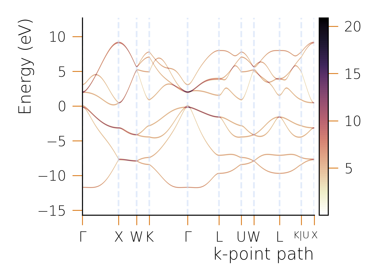
Band structure of bulk silicon along the standard k-path for diamond structures. The crystal
Hamiltonian is represented on a lattice through a Wannierization procedure. The band
structure is obtained by evaluating the Green's function in the k-vectors basis via
expansion in Chebyshev polynomials.#
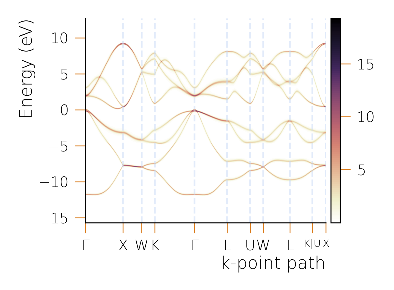
Band structure of disordered silicon along the standard k-path for diamond structures. The
system is modeled as mentioned in the pristine case. Disorder is represented by random onsite
potentials with a distribution of width 2 eV and the band structure is averaged over the
this distribution of disorder configurations. The calculations have been carried out on a
supercell of size 15x15x15.#
Onsite disorder introduces scattering induced broadening of the bands with a k-dependent
width.
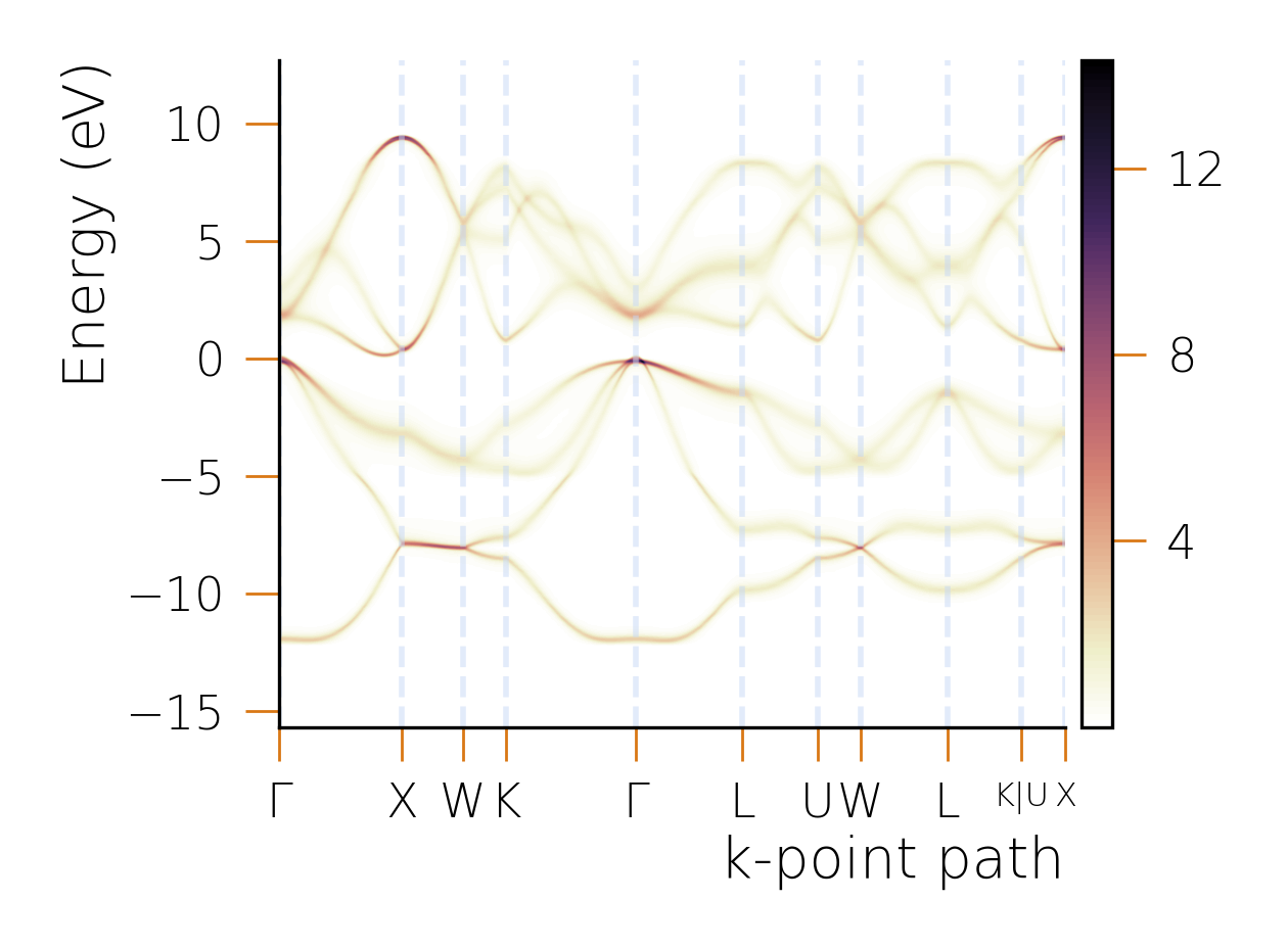
Band structure of disordered silicon as mentioned above. In this case the onsite disorder
distribution has width 4 eV. The supercell used is of size 20x20x20.#
Similarly with the previous case, onsite disorder induces a k-dependent band broadening, in
this case stronger, as expected.